MEMS Prototyping &
Process Development
We bridge the gap from academic proof-of-concept to commercial volume. Every project includes a digital process traveler to ensure your IP is portable and ready for seamless transfer to high-volume commercial foundries.
Bridging the Gap: We specialize in TRL 4–7
We take your academic-scale proof-of-concept and refine it into a robust, repeatable process ready for the commercial market. Our engineering team eliminates process drift before you scale.
Industry Verticals
Biotech & Microfluidics
SU-8 Masters • PDMS • Lab-on-a-Chip
Quantum & Photonics
E-Beam Litho • Dielectric Stacks
Medical Sensor Prototyping
Biocompatible Films • Encapsulation
IoT & Actuators
MEMS Sensors • DRIE • Piezoelectrics
Expert-Led Processing: Beyond the 'Black Box'
Standard foundries run fixed recipes. We run your recipe. Our senior process engineers understand the plasma physics inside the chamber, allowing for real-time tuning of bias power, gas ratios, and pressure to solve complex integration challenges that automated lines reject.
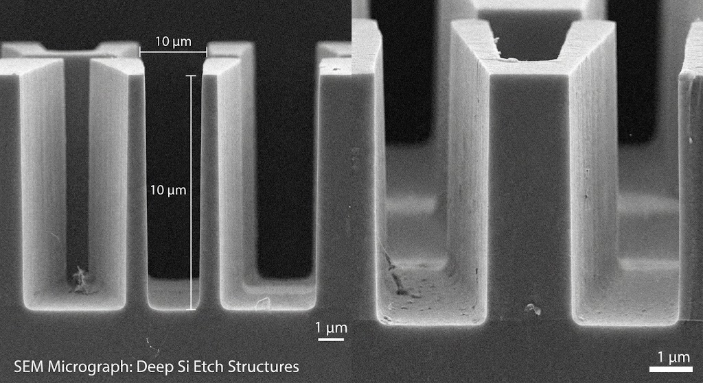
Fig 1: Cross-section SEM of high-aspect-ratio Bosch DRIE.
Deep Silicon Etch (DRIE)
We utilize the Bosch Process on STS Pegasus tools to achieve high-aspect-ratio (>50:1) structures with vertical sidewalls (90° ± 1°). Parameter ramping is used to control profile evolution, minimizing 'footing' at the buried oxide layer in SOI wafers.
Engineering Insight
"Scallop Control is critical for microfluidics. We can tune our switching cycles to reduce sidewall roughness to <50nm, ensuring smooth flow in micro-channels."
Thin Film Deposition
High-purity PVD and CVD for optical, electrical, and structural layers. We don't just deposit films; we tune them. By adjusting deposition frequency and temperature, we tailor the Refractive Index for photonics and control Mechanical Stress to prevent buckling.
The Stress Problem
"MEMS Failure #1 is Stiction and Curling. We characterize the stress of our Oxide/Nitride stacks to create 'Zero-Stress' released membranes that remain flat after sacrificial etching."
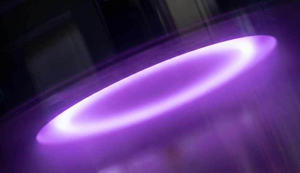
Fig 2: PECVD chamber during oxide deposition run.
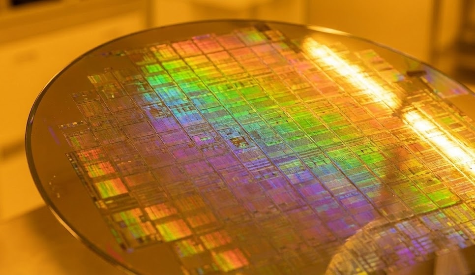
Fig 3: 6-inch silicon wafer post-lithography patterning.
Photolithography
Mix-and-match lithography strategies using Heidelberg Maskless (Direct Write) for rapid prototyping (0.7µm) and GCA Steppers for high-volume batch processing (0.5µm).
Alignment Edge
"Advanced backside alignment capabilities allow for precise double-sided patterning, essential for pressure sensors and micro-fluidic inputs."
Standard Process Specifications
Baseline tolerances for LNF toolsets (Best Effort).
Lithography
| Min Feature (Direct Write) | 0.7 µm |
| Min Feature (Stepper) | 0.5 µm |
| Alignment Accuracy | ± 0.15 µm |
| Front-to-Back Align | ± 1.0 µm |
Deep Silicon Etch (DRIE)
| Aspect Ratio | > 50:1 |
| Sidewall Profile | 90° ± 1° |
| Scallop Depth | < 50 nm |
| Selectivity to Resist | > 75:1 |
| Selectivity to Oxide | > 150:1 |
Thin Film Deposition
| Film Uniformity | < 3% |
| LPCVD Nitride Stress | < 250 MPa |
| PVD Base Pressure | < 5.0e-7 Torr |
| Available Targets | Au, Pt, Ti, Cr, Al, Ni |
Metrology & Inspection
| SEM Resolution | < 5 nm |
| Film Thickness Accuracy | ± 1 Å |
| Step Height Resolution | < 10 Å |
Unsure if your design fits these specs?
Don't guess. Submit your layout for a complimentary DFM (Design for Manufacturing) Feasibility Check before you commit to a full run.
Turnkey Logistics: Masks & Materials
We manage the supply chain to protect your lead times.
Mask Generation Services
Don't waste time managing mask vendors. Send us your GDSII/DXF, and we handle the data conversion, polarity checks, and procurement.
- Turnaround: Rapid 24-48 hour options.
- Types: Chrome (Quartz/Soda Lime) & Mylar.
In-Stock Substrates (Immediate Start)
We maintain an inventory of standard substrates to ensure your run starts Day 1.
- Silicon: 100mm/150mm (P/N, 1-10 ohm-cm).
- Glass: 100mm Borofloat 33 / Fused Silica.
- SOI: Device Layers 10µm - 50µm.
- Coated: In-stock Thermal Oxide & LS Nitride.
Sourcing Network
Need exotic substrates? We handle the procurement through our trusted network of specialty wafer vendors.
- Exotics: GaN, Sapphire, SiC, Piezo.
- Validation: Material compatibility pre-checks.
The Production Bridge Roadmap
- 1 Validation of baseline process recipes on industry-standard tools.
- 2 Refinement of critical dimensions (CD) and yield optimization.
- 3 Generation of a full Digital Process Traveler for foundry handover.
Scalability & The Path to Production
We don't just build your prototype; we build a scalable business. By utilizing industry-standard toolsets at the Lurie Nanofabrication Facility (LNF), we prioritize Foundry-Compatible processes. When your design is validated, we provide you with a full, transparent Digital Process Traveler to ensure a seamless transfer to high-volume commercial foundries.
Quality Assurance & IP Protection
Rigorous process control in a secure US-based environment.
Process Control
- Digital Run Sheets: Every lot is tracked via a comprehensive Digital Traveler, recording tool parameters, etch times, and operator logs for full traceability.
- Incoming QC: All substrates and masks undergo strict microscopic inspection upon arrival to verify spec compliance before processing begins.
- Metrology Gates: Critical process steps (Litho, Etch, Dep) are gated by mandatory metrology checks. We do not proceed to the next step until tolerances are verified.
Data Security
- US-Based Operations: All fabrication and data storage occur strictly within the United States. Your IP never crosses borders.
- Secure Handling: Design files are stored on encrypted, access-controlled servers. We strictly enforce "Need-to-Know" access protocols for our engineering staff.
- Non-Compete Assurance: As a pure-play foundry, we do not develop internal products that compete with our clients. Your success is our only business.
Process Architecture Led by Published Experts
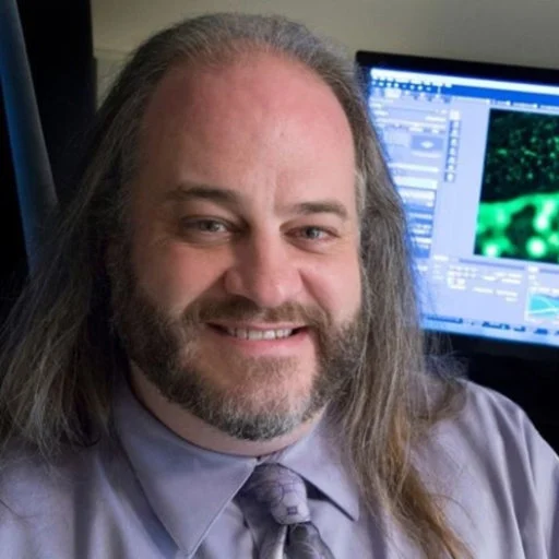
Christopher Frewin
Chief Process Architect & Lead Inventor
Christopher brings over a decade of specialized expertise in micro-fabrication, with a focus on neural interfaces, high-aspect-ratio MEMS, and biocompatible material integration. His work bridges the gap between novel academic research and commercially viable manufacturing.
As a holder of multiple patents and a widely cited researcher, he oversees all process travelers at Cleanroom Fab, ensuring that every project is engineered for both physical robustness and scalable yield.
Key Technical Expertise
Flexible Engagement Models
From single process steps to full device integration.
Unit Process Service
- Best For: Overflow capacity & single steps.
- Scope: Lithography, Etch, Deposition, or Metrology only.
- Lead Time: 1–2 Weeks.
- Deliverable: Processed Wafers + Metrology Report.
Pricing
Machine Hourly + Eng. Time
Feasibility & Design Review
- Best For: Validating new designs before fabrication.
- Scope: DFM Review, Material Compatibility Check, Mask Layout Review.
- Lead Time: 5 Business Days.
- Deliverable: Written Feasibility Report & Draft Process Traveler.
Pricing
Fixed Fee Packages Available
Full Custom Prototyping
- Best For: TRL 4–7 Device Development.
- Scope: End-to-end fabrication (Mask procurement to Dicing).
- Lead Time: 4–8 Weeks.
- Deliverable: Functional Devices, Final Run Sheet, & IP Handover.
Pricing
Project-Based Quote
Technical Knowledge Base
Deep-dive into our commercial operational model, technical capabilities, and IP protocols.
| Capability | Specification |
|---|---|
| Lithography | 0.7µm Min Feature (Maskless); 0.5µm (Stepper) |
| DRIE Etch | >50:1 Aspect Ratio; Bosch Process |
| Deposition | Au, Pt, Al, Ti, Cr, Ni, Oxide, Nitride, Poly-Si, ALD |
| Substrates | 100mm (4") and 150mm (6") Silicon, SOI, Glass |
- Single-Step Runs: 1–2 weeks.
- Patterned Devices: 4–8 weeks (Complexity Dependent).
- Metrology: Every run includes a verification report featuring Stylus Profilometry, Ellipsometry, and/or SEM inspection images to confirm critical dimensions.
Start a Fabrication Run
Submit specifications for a feasibility review and production roadmap.